ASML’s 2026 High-NA EUV Tools Spark Global AI Chip Race
ASML has officially confirmed its High-NA EUV lithography systems are ready for mass production, enabling the fabrication of next-generation AI chips with unprecedented precision. This milestone marks a pivotal shift in global semiconductor dominance, with major tech firms racing to integrate the technology into their chip roadmaps.

ASML’s 2026 High-NA EUV Tools Spark Global AI Chip Race
summarize3-Point Summary
- 1ASML has officially confirmed its High-NA EUV lithography systems are ready for mass production, enabling the fabrication of next-generation AI chips with unprecedented precision. This milestone marks a pivotal shift in global semiconductor dominance, with major tech firms racing to integrate the technology into their chip roadmaps.
- 2Amsterdam, Netherlands — ASML Holding N.V., the Dutch semiconductor equipment giant with a near-total monopoly on extreme ultraviolet (EUV) lithography, has announced that its next-generation High-NA EUV tools have cleared all technical and operational hurdles and are now certified for mass production in 2026.
- 3This breakthrough marks the official start of a new era in artificial intelligence chip manufacturing, with profound implications for global tech supply chains, national security, and economic competitiveness.
psychology_altWhy It Matters
- check_circleThis update has direct impact on the Sektör ve İş Dünyası topic cluster.
- check_circleThis topic remains relevant for short-term AI monitoring.
- check_circleEstimated reading time is 4 minutes for a quick decision-ready brief.
Amsterdam, Netherlands — ASML Holding N.V., the Dutch semiconductor equipment giant with a near-total monopoly on extreme ultraviolet (EUV) lithography, has announced that its next-generation High-NA EUV tools have cleared all technical and operational hurdles and are now certified for mass production in 2026. This breakthrough marks the official start of a new era in artificial intelligence chip manufacturing, with profound implications for global tech supply chains, national security, and economic competitiveness.
How High-NA EUV Transforms AI Chip Production
ASML’s High-NA EUV systems use a numerical aperture of 0.55 to etch circuit patterns as small as 8 nanometers, delivering a 1.8x improvement in lithography resolution over previous EUV tools. This enables chipmakers to pack more transistors onto a single die without increasing physical size — a critical advancement for AI accelerators demanding extreme computational density.
- Lithography resolution: 8nm pattern capability
- Wavelength: 13.5nm extreme ultraviolet light
- Throughput gain: 1.8x faster wafer processing
- Chip yield improvement: Up to 25% higher than 7nm EUV
Why Resolution Matters for AI Accelerators
AI chips like NVIDIA’s upcoming Blackwell architecture rely on dense 3D chiplet designs and advanced packaging. High-NA EUV enables precise patterning of these microstructures, reducing signal delay and power loss — key for achieving 40% higher performance-per-watt in 2026 models.
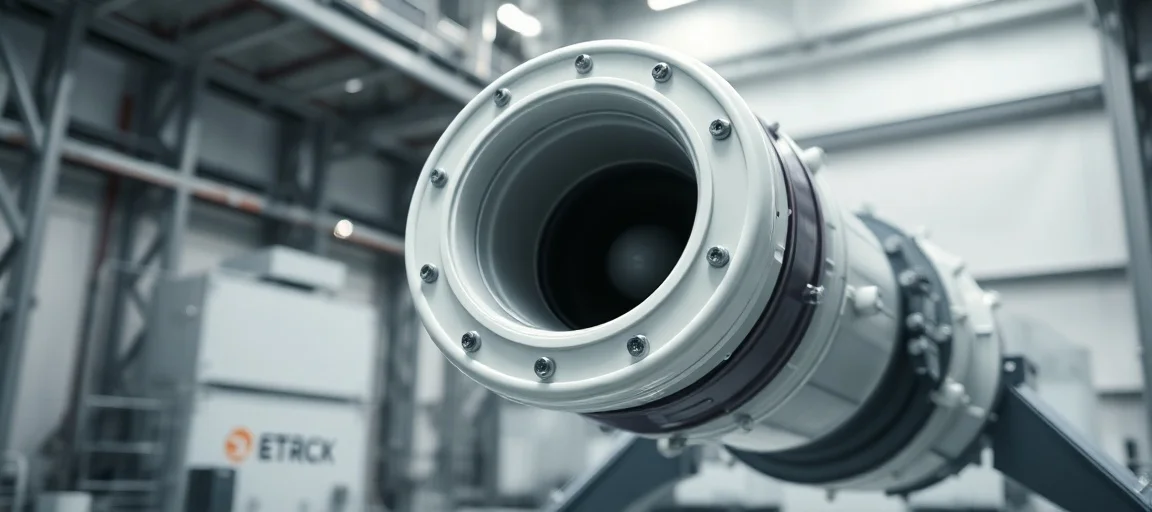
From Pilot to Production: Real-World Deployment
ASML’s first production units have been shipped to TSMC’s Fab 18 in Hsinchu, Taiwan, and Samsung’s Hwaseong facility in South Korea. Intel’s Arizona plant is expected to receive its first unit by Q3 2026, accelerating its chip revival strategy.
TSMC and NVIDIA’s Race to Adopt New Tools
NVIDIA, AMD, and Intel have all confirmed integration of High-NA EUV into their 2026–2027 product roadmaps. NVIDIA’s Blackwell GPUs will be the first AI accelerators manufactured using this technology, targeting enterprise AI and generative AI workloads with unprecedented efficiency.
According to Gartner, by 2028, over 70% of enterprise AI chips will be produced using High-NA EUV, making wafer fabrication capacity a strategic bottleneck.
Chiplet Design and 3D Stacking Enable Breakthroughs
High-NA EUV enables precise interconnects for chiplets and silicon interposers, allowing AI systems to scale compute without hitting thermal or power walls. This is critical for training trillion-parameter LLMs.
The Global Semiconductor Power Shift
With each High-NA EUV machine costing over $350 million and requiring seismic isolation and climate-controlled facilities, access to this technology is tightly controlled. The U.S. and EU have accelerated export controls to limit China’s access, adding two Chinese firms to the Entity List for attempting to acquire components via intermediaries.
ASML’s Dutch operations remain the sole global source, reinforcing Europe’s pivotal role in the AI hardware ecosystem. As geopolitical tensions rise, securing supply chains for EUV tools has become a national priority.
What’s Next? The Road to 2nm and Beyond
Industry analysts expect High-NA EUV to enable 2nm and sub-2nm nodes by 2027–2028. TSMC has already begun R&D on High-NA EUV+ for 1.4nm nodes, while Intel targets 18A (1.8nm) process with this technology.
Expert Insight: ASML CEO Peter Wennink
"We are not just building machines — we are building the foundation for the next decade of artificial intelligence," said ASML CEO Peter Wennink in a recent investor call. "The ability to pattern at this scale defines who leads in AI — and who follows."